PSK is a digital modulation technique defined as the process of shifting the phase of the carrier signal between two levels, depending on whether 1 or 0 is to be transmitted.
Phase shift keying is a digital modulation process which conveys data by changing the phase of a reference signal. The modulation occurs by varying the sine and cosine inputs at a precise time.
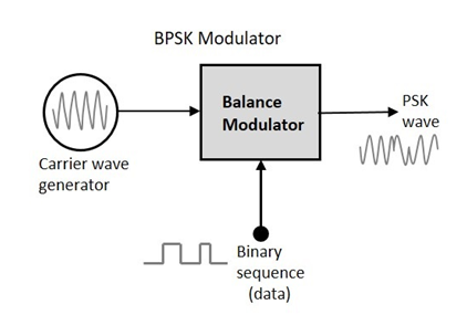
Any digital modulation scheme uses a finite number of distinct signals to represent digital data. PSK uses a finite number of phases; each assigned a unique pattern of binary digits.
Usually, each phase encodes an equal number of bits. Each pattern of bits forms the symbol that is represented by the particular phase. The demodulator which is designed specifically for the symbol-set used by the modulator, determines the phase of the received signal and maps it back to the symbol it represents, thus recovering the original data.
This requires the receiver to be able to compare the phase of the received signal to a reference signal-such a system is termed coherent.
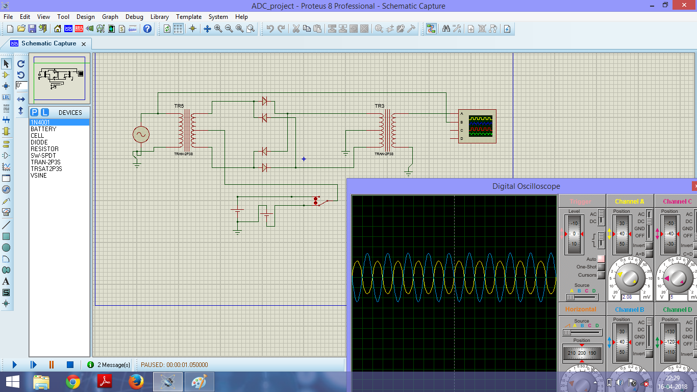
The heart of most PSK Modulators is the balanced modulator. This circuit allows the phase of a carrier sine wave (fc) to be altered by a modulating digital signal. It is used to illustrate the concept behind balanced modulators. By and large, most balanced modulators today are made from semi conductor devices to avoid the expense, band limitations, and associated magnetic distortions and interference inherent in transformers.
WORKING-
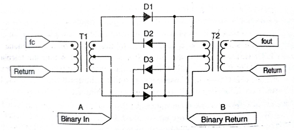
The reference frequency (fc) is applied to T1 and is coupled through the secondary winding to the diode D1 and D2 on the high side and D3 and D4 on the return side. The in-phase relationship between the input (primary winding) side of the transformer and the output side (secondary winding) is indicated by the dots at the top side of both transformers.
On the return side of the secondary, the signal is 180 degree out of phase with dotted reference point. The digital data stream is applied to the centre taps of T1’s secondary and T2’s primary. The current level supplied by the digital circuit is enough to cause the diodes to turn on when the
correct polarity is applied.
As a point of reference, logic 1 is selected to be positive at input A and negative at input B. This forward biases diodes 1 and 3 and turn off diodes 2 and 4.
Reversing the polarity at inputs A and B to represent a zero, turns on D2 and D4 while back biasing D1 and D3.This time fc is directed to the opposite (non dotted) end of T2. The output signal coupled to T2’s secondary is 180 degree out of phase with fc at the input.
The magnitude of the vectors used on this and subsequent phase diagram (except QAM) is of unit length. This is easily acceptable since these devices are modulating phase while keeping amplitude and frequency constant.
·
Bit logic 1 is in phase with the given input signal
·
Bit logic 0 is 180 0 out of phase with the given input signal